In the race to build a computer that mimics the massive computational power of the human brain, researchers are increasingly turning to memristors, which can vary their electrical resistance based on the memory of past activity. Scientists at the National Institute of Standards and Technology (NIST) have now unveiled the long-mysterious inner workings of these semiconductor elements, throwing light on their ability to act like the short-term memory of nerve cells.
One nerve cell’s proficiency at signaling another depends on how often the cells have communicated in the recent past, so a memristor’s resistance also depends on the amount of current that recently flowed through it. Moreover, memristors retain that memory even when electrical power is switched off.
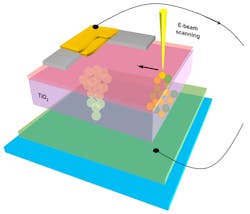
An electron beam impinges on a section of a memristor, a device whose resistance depends on the memory of past current flow. As the beam strikes different parts of the memristor, it induces different currents, yielding a complete image of variations in the current throughout the device. Some of these variations in current indicate places where defects may occur, indicated by overlapping circles in the filament (titanium dioxide), where memory is stored.
But despite the keen interest in memristors, scientists have never had a detailed understanding of how they work, and have yet to develop a standard toolset to study them.
Now, NIST scientists have stepped in to create such a toolset and used it to more deeply probe how memristors operate. Their findings could lead to more efficient operation of the devices and suggest ways to minimize current leaks.
To explore the electrical function of memristors, the team aimed a tightly focused beam of electrons at different locations on a titanium dioxide memristor. The beam knocked free some of the device’s electrons, which formed ultrasharp images of those locations. The beam also induced four distinct currents to flow within the device. The team determined the currents were associated with the several interfaces between materials in the memristor, which consists of two metal (conducting) layers separated by an insulator.
The team knows exactly where each of the currents comes from because it controlled the location of the beam inducing those currents.
In imaging the device, the team found several dark spots—regions of enhanced conductivity—which indicated places where current might leak out of the memristor during normal operations. These leak pathways were outside the memristor’s core where it switches between low and high resistance levels, a potentially useful trait in an electronic device. The finding suggests that reducing the size of a memristor could minimize or even eliminate some of the unwanted current pathways. Although researchers had suspected that might be the case, they had lacked experimental guidance about just how much to reduce the size of the device.
Because the leakage pathways are tiny, involving distances of only 100 to 300 nanometers, the team believes there probably aren’t going to be any big improvements until it reduces the memristor’s dimensions on that scale.
To their surprise, the researchers also found the current that correlated with the memristor’s switch in resistance didn’t come from the active switching material at all, but the metal layer above it.
The most important takeaway from the memristor study is that you can’t just worry about the resistive switch—the switching spot itself. You have to worry about everything around it. The team’s study should lead toward developing a better feel for how to engineer and build memristors.


