MEMS May Lead to Chip-Based “Personal” Electron Accelerator
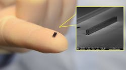
Physicists and engineers are familiar with costly high-energy electron-particle accelerators, and their mile-long structures needed to achieve mega-electron-volt (MeV) energy levels. But there’s a new approach being explored, once again leveraging the ability of MEMS technology to create ultra-small channels and structures. It’s a similar situation to the diverse efforts dedicated to MEMS-based gyroscopes, laser-power measurement, resonators, and spectrometers (see “Related” items below).
The Accelerator on a Chip International Program (AChIP) funded by the Gordon and Betty Moore Foundation in the U.S., is focused on creating a silicon-based electron accelerator. (A related project is attempting to build an “accelerator in a shoebox” with more ambitious goals under different constraints and tools). The goal of this multidisciplinary, multi-institution program, which has funding until 2020, is to produce pulses of electrons with one MeV of energy from the chip, developing femtosecond to attosecond (10-15 to 10-18 second) pulses.
In their paper “Alternating-Phase Focusing for Dielectric-Laser Acceleration” published in Physical Review Letters, electrical engineers in the project’s accelerator physics group at TU Darmstadt have developed a design for a laser-driven electron accelerator so small that it could, in theory, be fabricated on a silicon chip.
The design uses a glass and silicon structure at its core with an external laser as an energy source instead of the microwave generator of conventional accelerators. The high electric-field strength of glass means that the particle acceleration rate can be increased; therefore, the same amount of energy can be transferred to the particles within a shorter physical space. The result is an accelerator that’s an order-of-magnitude shorter than traditional accelerators delivering the same energy.
Of course, building this is easier said than done, as the vacuum channel for the electrons on a chip must be very small which, in turn, requires that the electron beam be very sharply focused. The traditional magnetic-focusing approach used in existing accelerators is too weak to achieve this, so an entirely new focusing method needs to be developed if the accelerator-on-a-chip is to become reality.
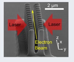
1. The dual-pillar structure fabricated in silicon uses laser-based optical phase control to focus the electron acceleration and deceleration zones.
This is where the convergence of lasers, electronics, and deep physics becomes even more complex, advanced, and subtle. The AChIP sub-group at Technische Universität Darmstadt (TU Darmstadt) in Germany has developed a different solution, using the fields of the source laser to focus the electrons in a channel only 420 nm wide (Fig. 1). Their efforts are just one facet of this highly complex, broadly based, collaborative university project. Additional information is available in a detailed slide presentation “Photonics-based laser-driven particle acceleration: from proof-of-concept structures to the accelerometer on a chip.”
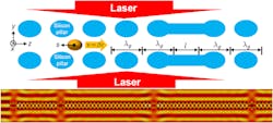
This MEMS-based accelerator implements a two-dimensional design that’s compatible with conventional silicon fabrication, unlike the electron dynamics of a magnetic-based accelerometer. It uses a technique called alternating-phase focusing (APF), which initiates laser-driven alternation of focusing and defocusing along the two directions in the plane of the chip’s surface (Fig. 2). Although somewhat counterintuitive—but fully supported by physics—this creates particle stability along both longitudinal and transverse axes and keeps the electrons where they should be.
2. Schematic view of a dual-pillar dielectric-laser acceleration (DLA) structure and a particle bunch around a reference particle (top); simulation of the longitudinal time-harmonic electric field (bottom).
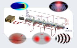
The APF technique discussed here can also be used to produce the bunching needed to inject electrons into the accelerator structure. The creation and removal of sinusoidal energy also yields extremely short (attosecond) bunch lengths with a low spreading of electron energies (Fig. 3).
3. A schematic of the complete electron accelerator, showing the buildup of energy and pulsing at each sequential stage.
The non-research uses for this device, if and when it becomes a practical reality, may be unclear at this time, but that doesn’t matter. After all, commentators quipped that the laser was “a solution looking for problems to solve” when it first demonstrated. One possible use is in medical treatment, as a combined accelerator-endoscope that uses electrons to irradiate tumors deep within the body.


