Applying Metal Bellows in Ultrahigh Vacuums
This file type includes high-resolution graphics and schematics when applicable.
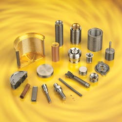
Semiconductor manufacturing facilities and other high-vacuum environments have a reputation for being tough on components. These settings involve exposure to corrosive conditions or media (gases and/or liquids), and the equipment used in such extremes has an extremely low tolerance for contamination. Metal bellows find wide use in these industries because of their repeatable positioning capabilities and ability to work in severe conditions.
A metal bellows typically has the physical form of a flexible, springlike accordion. But that changes once it fills with a liquid or gas under atmospheric or vacuum conditions and its ends are sealed. Then the bellows will be extremely sensitive to a variety of forces, providing a predictable, repeatable, dynamic response.
Within the realm of semiconductor wafer processing, UHV (ultrahigh vacuum), or ultrahigh-purity processing, vacuum and pressure bellows can carry out a variety of functions. For example, they can be found in semiconductor clean rooms where they can establish and maintain certain atmospheres. In optical devices, they can precisely position filters and lenses used to direct light during the process of semiconductor manufacturing. Additionally, they can be used as flexible, hermetically sealed feedthroughs in process chambers to maintain high-pressure or vacuum while an operator positions various apparatus during the manufacture of semiconductor chips.
Several aspects of the processing environments that characterize UHV processes can create distinct challenges for metal bellows. Specifically, such bellows must typically be engineered with miniature dimensions (length, diameter, and wall thickness) and exacting performance specifications for high reliability. In addition, they must be engineered with low spring rates (a measure of the pounds of force necessary to compress the bellows) and maximum leak tightness (to ensure absolutely no fluid or gas leaks out of the sealed bellows or leaks in).
Similarly, the demanding nature of most semiconductor processing environments dictates that metal bellows can be fabricated from special materials. For example, some semiconductor applications require a bellows manufactured from a nonmagnetic material. In others, the existence of corrosive process gases can impose strict material requirements or constraints. In general, metal bellows are produced using one of three main techniques: electrodeposition (also called electroforming), edge welding, and hydroforming. Each technique has advantages and disadvantages. Among the manufacturing methods available, electrodeposition and edge welding are both widely used to produce the bellows needed for semiconductor manufacturing and UHV applications.
Electrodeposited (also called electroformed) bellows are produced by plating metal (most often copper, nickel, or a nickel alloy) onto a bellows-shaped form (mandrel), and then removing the mandrel using chemical or physical methods. These techniques can let manufacturers carefully control the bellows wall thickness and produce bellows with tiny diameters and super-thin walls (on the order of 0.0010 to 0.00010 in.). At these dimensions, the resulting miniature bellows are extremely sensitive and well suited for precision instrument applications. They can also provide large deflections in response to the application of small forces (as low as 4 g).
If electrodeposited nickel alone is not an option (for instance, when there are issues that could arise from exposure to corrosive agents), then gold or Parylene-C could be considered for use as a surface coating. In the case of a nonmagnetic bellows, electrodeposited nickel, being ferromagnetic, will be ruled out. Then an alternative such as copper may be a possibility.
In highly specialized cases, nickel may be ruled out in favor of copper. Such situations might arise when the device also functions as a heat sink using all copper and no nickel. A key advantage of electrodeposition is the ability to produce bellows having highly sophisticated parameters. Electrodeposited bellows can have miniaturized overall dimensions, as small as 0.020 in. in diameter, and exceedingly thin wall thicknesses down to 0.00010 in. They can also have extremely high cycle life and a low leak rate (down to 1 × 10⁻⁹ std. cc He/sec, as verified by mass spectrometer — a leak rate that translates to 1 cc in 32 years). Plus, they can have a compression stroke, in some special cases, up to 60% of their free length.
This combination of attributes makes electrodeposited bellows good candidates for extremely sensitive, precision instruments. Similarly, the fact that they are seamless and nonporous is important in semiconductor-related applications where the potential for contamination is a key consideration.
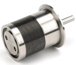
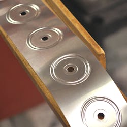
By comparison, edge-welded bellows can be made from more than a dozen materials including stainless steel, Inconel, Hastelloy, titanium, and others. They are produced by welding metal diaphragms that have been stamped from strip material using plasma, laser, arc, or electron-beam welding methods. Compared to electrodeposited bellows, edge-welded bellows are stronger and more robust. However, this edge welding can’t produce bellows with extremely small diameters or thin walls.
Compared with those produced using the other fabrication methods, edge-welded bellows have the highest stroke length (reaching 90% of their free length) and enjoy excellent compression capabilities, allowing for a lot of expansion and contraction during operation. And with a greater variety of metallurgical options available, edge-welded metal bellows can also withstand exposure to extremes in liquid and gas media and temperatures.
Design considerations
When it comes to specifying metal bellows, compatibility issues will dictate metal selection. In many semiconductor-production processes the presence of corrosive gases creates specific requirements or constraints that limit the kind of metal that will work as an engineered bellows. While the final specification will be dictated by site-specific criteria, the list of acceptable materials for electrodeposited bellows typically includes nickel, copper, and gold in any combination. For edge-welded bellows, additional materials include AM 350, types 316L, 304L and 347 stainless steel, Inconel 718/625, Hastelloy 276C, Haynes 242, and Titanium grades 1–4 (ASTM-B265).
Electron-beam welding can be used to eliminate the use of solders and epoxies. In many industrial applications, solders and epoxies connect the metal bellows within the machine assembly. However, both these materials tend to produce potential contaminants (via off-gassing) that are unacceptable within pristine semiconductor-manufacturing environments. As a result, such applications tend to require welded connections to join the bellows to the machine assembly. While lasers are widely used for this purpose, bellows made from electrodeposited nickel cannot be laser-welded directly to steel parts.
To expand the versatility of electrodeposited nickel bellows, a small transition piece of 304L and 316L stainless steel can be e-beam welded to the bellows. Then that steel transition piece can be laser-welded to steel parts within the machine assembly. Electron-beam welding takes place using highly automated computer controls, and this welding technique imparts only localized energy to the work piece, minimizing distortion of thin parts. It also produces exceptionally clean welds in applications that cannot tolerate contamination or volatile outgassing. Such a workaround solution would require that sufficient space is available where the bellows assembly must fit, or would require special design considerations at the time the bellows is ordered.
Proper manufacturing can ensure tight spring rate tolerances and minimal stroke. Metal bellows used in many semiconductor applications must meet exacting design tolerances. With proper manufacturing, bellows can be produced with spring rates controlled to ±10%. In some applications gold flash (0.000050 in., ASTM B 488) can be applied over ultrathin bellows walls to further boost leak tightness and resistance to corrosion.
It should be noted that semiconductor processes involve stringent cleaning protocols that have a direct impact on the bellows manufacturing technique and/or the material. Many cleaning protocols involve ultrasonic cleaning in a fluid medium for any components that go into semiconductor equipment.
When specifying a bellows, the OEM must inform the bellows vendor about the specific cleaning protocols because these will directly impact the manufacturing technique and materials the bellows can use. For instance, electrodeposited bellows can be cleaned using ultrasonic methods — but only as long as the ultrasonic frequency does not exceed 40 kHz. Otherwise the bellows will be damaged.
Small size requirements are also critical. As the demand for miniature manufacturing rises, device geometry continues to shrink. This creates ongoing challenges in terms of tight space constraints. Today’s advanced electrodeposited technology lets metal bellows be manufactured in sizes ranging from 0.020 to 12 in diameter.
Edge welding can produce bellows for semiconductor applications in a range of metals and dimensions. Today’s advanced edge welding techniques produce bellows in diameters ranging from 0.396 to 36 in. and in a range of metals including Inconel, Hastelloy, AM350, titanium or stainless steel for semiconductor applications. In instances such as UHV applications, stainless steel is the only material option. However, edge-welded bellows face some size limitations that are best covered in discussions with the bellows supplier.
Resources:
Servometer


