Katie Sautter, a postdoctoral researcher at the U.S. Department of Energy’s (DOE) Argonne National Laboratory, researches quantum materials as part of Q-NEXT, a DOE National Quantum Information Science Research Center. She develops materials that will be used in quantum communication devices.
“Quantum devices have an enormous range of potential applications in cybersecurity, computing, data communications and lasers—quantum engineering can take all of these in a direction that can’t be taken using traditional methods,” said Sautter, who works with Q-NEXT in Argonne’s Nanoscience and Technology division.
Q-NEXT researchers working under the guidance of Argonne scientist, University of Chicago Professor and Q-NEXT Chief Technology Officer Supratik Guha, are creating materials for quantum memories that can be built on silicon chips.
Sautter’s specialized expertise in materials will contribute to devices that hold quantum memories. These memories are earmarked for devices known as quantum repeaters.
Quantum repeaters enable the transmission of quantum information over longer distances of optical fiber. Signals become weaker as they travel along the fiber. The quantum repeater repeatedly “stitches” the signal back together so that the information can be conveyed along the fiber’s length. Without them, the signal dissipates before it arrives at its destination.
Although quantum repeaters are only in the design stage, they hold great promise for quantum communication. Quantum memory devices could also work in the telecommunication band of frequencies, making them compatible with today’s fiber-optic networks.
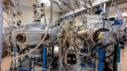
One of the tools in Suatter’s arsenal is a specially designed molecular beam epitaxy machine (MBE) system in Guha’s laboratory. The machine is playfully described as a “steampunk-meets-sci-fi-looking tool.” The MBE can build enough material for a compact, high-performance device within a matter of hours.
The MBE process ensures the production of pure materials, as it is not dependent on the use of preparatory chemicals to jumpstart a process.
Sautter and her colleagues will focus on building oxide heterostructures—materials with layers made of two or more oxygen compounds—as their structural arrangements make them ideal for quantum memory processing.
WISE Facts About Sautter
- Her path to quantum engineering started at Pennsylvania State University, where she studied materials science and engineering.
- An internship at the DOE’s Colorado-based National Renewable Energy Lab, working with the high-efficiency solar-cell team, inspired her decision to pursue her doctorate.
- Sautter received her Ph.D. in materials science and engineering in May 2021 from Boise State University.
- She is an expert in a special material-growth process: Individual layers of atoms are meticulously stacked on top of one another using the aforementioned molecular beam epitaxy machine. She used the university’s MBE to make quantum dots, bits of matter only thousands of atoms wide. Five thousand dots could fit along the width of an average human hair.
Editor's Note: Machine Design’s Women in Science and Engineering (WISE) hub compiles our coverage of gender representation issues affecting the engineering field, in addition to contributions from equity seeking groups and subject matter experts within various subdisciplines. Click here for more.


