What Methodology Best Fits 2D-Material Fabrication?
Not all 2D materials are a single atomic layer or an elemental material like graphene (C). These materials offer strong covalent bonds (sharing electron pairs between atoms) that enable the formation of atoms on a layered plane. The layers are loosely bound to each other via weak van der Waals interactions.
This file type includes high resolution graphics and schematics when applicable.
Graphene has been known about for decades, so why is it receiving press now? First, graphene was actually produced in a lab only 12 years ago in 2003, so it’s relatively new and there’s still much to discover. One reason might also be that its revenue was $9 million in 2012, according to Lux Research. That’s an impressive number, considering the newness of the material, or that a commercial market has yet to be defined.
Ultimately, the attention seems to be centered on graphene’s potential applications. Much of the work is either theoretical or experimental to gain insight into the material’s potential applications. However, the vast array of possible applications, ranging from coatings and polymer fillers to electronics, has caught the interest of many people in and outside of nanoscience.
2D Materials
Jonathan Coleman, professor of chemical physics at Trinity College, said he and his team have looked at over 20 different types of 2D materials. New methods and processes are starting to produce graphene on a larger scale to make it more commercially available. Coleman believes this will be the year when we find out which industry will adopt the material and inevitably show us its commercial applications.
Graphene (C) is the strongest material discovered to date. It has strong carbon bonds, with a tensile strength of 18855 ksi (130 GPa). For comparison, A36 steel’s tensile strength ranges from 59 to 80 ksi (0.4 to 0.55 GPa). It weighs ~ 2.52e-6 oz/ft2 (0.77mg/m2), and is only an atom thick. Graphene is also more electrically conductive than copper. This may lead its use in high-frequency electronics applications such as high-power transmitters, or to create flexible, high-performance electrodes for batteries. Graphene’s high surface area could also improve capacitor charging and discharging rates.
Another type of material is the family of transition metal di-chalcogenides (TMD) that might find use in batteries and thermoelectric generators. MoS2 is one of these materials and, unlike graphene, has a bandgap. This means it can be turned off (on/off ratio 1x10⁸), but still offers a high electron mobility. As a result, it potentially becomes more attractive in applications that require semiconducting behavior, such as transistors.
Philip Feng, an engineering professor at Case Western Reserve University, says the bandgap for MoS2 depends on the number of its atomic layers. Bandgaps can also be continuously tuned by mechanical strain. MoS2 has special optical properties in terms of transparency, absorption, and refractive indices that might lead to its use in optical sensors. With an ultra-high flexibility and fracture strain limit (~20% to 25%, similar to graphene), in addition to its piezoelectricity, MoS2 should be a good candidate for electromechanical sensors.
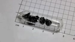
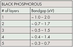
Coleman said that among many types of 2D materials, black phosphorus (or phosphorene) seems to have captured people’s interest (see the table). It’s a single layer of phosphorus, and has a controllable bandgap of 1.5 eV for a monolayer to 0.59 eV for a five-layer sample.
A controllable bandgap, made possible by adding or removing layers of material, is important when designing electronics. A small gap would be desirable when building semiconductors and transistors. However, higher-power electronics, like some analog and radio-frequency devices, may demand a higher bandgap.
The bandgap is also direct, meaning it emits light. By changing the bandgap, engineers can change the color of the emitted light. Thus, it’s ideal for photodetectors and solar cells. When asked if black phosphorus could be used in quantum dots for televisions, Coleman said, “It is far too soon to make assumptions as to where black phosphorene will be adopted.”
Feng added, “Black phosphorus is also anisotropic in all electrical, optical, and mechanical properties. This means its properties can change based on its orientation along the x-axis or y-axis. With high electron mobility in both n- and p-type transistors, it could be used to make CMOS phosphorene devices.” This is also true for MoS2.
Black phosphorous does degrade in water and oxygen. This may not be a problem, though, because large quantities of it can be made with a liquid exfoliation process. In addition, experiments with a solvent of N-cyclohexyl-2-pyrrolidone (CHP) revealed prevention of degradation from water and oxygen. There are also methods to encapsulate phosphorene layers in protective coatings to prevent degradation.
Making 2D Materials
Many processes can be used to create 2D materials, four of which are discussed in this article: chemical vapor deposition, micromechanical cleavage, liquid exfoliation, and dry exfoliation. There are two general types of approaches—top-down and bottom-up methods. The top-down approach is like exfoliation, in which a bulk material gets separated into nanosheets. The bottom-up approach adds layers onto a substrate, or grows them from smaller atomic or molecular components.
Thin films can be grown using chemical vapor deposition (CVD). Various types of CVD processes are able to produce an array of materials, including 2D materials. The details of CVD can be rather complex, but the basic process involves gas-phase precursors deposited onto a substrate in a reaction chamber. CVD methods have been used for several decades to make thin films in the semiconductor industry.
Several important factors must be considered when selecting a type of CVD process to produce a material. They include cost and chemistry, along with desired qualities and properties of the resulting material.
Fortunately, for elemental materials like graphene, CVD growth should be more straightforward than materials with a more complex chemistry. Graphene can be grown using liquid, gas, and solid carbon-containing precursors. Two CVD processes that work well with making graphene are plasma-enhanced CVD and thermal CVD. Plasma-enhanced CVD is particularly beneficial because it’s also one of the least expensive methods. A range of pressures and substrates can be used when producing 2D materials in different growth processes and aid in moving them into a commercial market through mass production.
Qing Hua Wang, assistant professor of materials science at Arizona State University, mentioned that CVD of graphene on copper foil substrates is a promising technology used by companies like Samsung and IBM. Commercial applications that could arise from bottom-up-grown graphene include transparent conductors that exploit graphene’s broadband optical transparency, electrical conductivity, and mechanical properties. Other promising applications for top-down-exfoliated graphene include conductive inks and printable materials.
“The most promising methods for producing graphene at a scale appropriate for industrial applications would likely be CVD growth and liquid-phase exfoliation,” said Wang.
Mechanical cleavage, also known as micromechanical exfoliation, uses adhesive tape to pull apart layers of bulk graphite to obtain single atomic layers that are transferred to a supporting substrate. This method was utilized by Andre Geim and Konstantin Novoselov in their experimental work showing graphene’s unique properties (for which they won the Nobel Prize). This method produces very high-quality graphene, but has very low yield and cannot be scaled up for industrial applications.
In addition, electrostatic or electromagnetic forces can be used to split the bulk material into nanosheets. Such methods can be performed in air, a vacuum, or inert environments. These processes, including mechanical cleavage, are otherwise known as dry exfoliation.
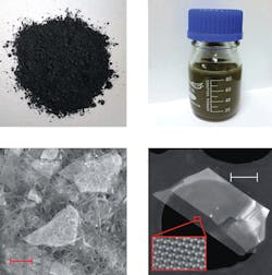
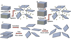
On top of that, scientists developed a new process in which large amounts of nanosheets can be produced in a liquid-exfoliation process. It uses amide solvents such as N-methyl-2-pyrrolidone, N-cyclohexyl-2-pyrrolidone, and in some cases, isopropanol alcohol. The surface of the bulk material is weakened by the solvent, and then subjected to ultrasonic frequencies that displace or exfoliate nanometer-thick sheets from the bulk material. A centrifuge removes unexfoliated material.
Liquid exfoliation can make nanometer-thick sheets of black phosphorous. In early experiments, the standard was 1,000 rpm for 180 min to yield stable nanosheets of black phosphorous. These experiments also revealed that it was possible to change the centrifuge’s speed to produce layered sheets in different sizes. Liquid exfoliation could also be scaled up for mass production, according to Trinity College’s Coleman.
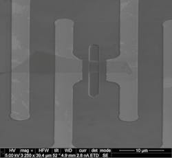
There’s a dry-transfer method that doesn’t generate nanosheets, but rather applies them to make electronic devices and mechanical sensors. It’s shown the ability to produce pristine MoS2 field-effect transistors (FETs) without additional wet processes.
The process initially employs the conventional wafer-scale process to pattern the electrodes, trenches, and other features. Then it dry transfers the 2D crystals on top, with alignment, to form the devices. This does allow for post processes to be administered and, in the case of thermal annealing, can even improve device performance.
The dry-transfer process is clean, easy, and can produce high-quality devices. It works well for the fabrication of transistors, suspended transistors, and other nanoelectromechanical devices.
The goal in mass-producing 2D materials is to take advantage of unique physical properties found in these atomically thin materials, and to make them in a form that’s easy to process with existing industrial methods. A number of challenges still must be overcome in order to produce large, atomically uniform 2D layers, but the production of graphene for a commercial mass market seems inevitable.
Many of the mentioned processes have reel-to-reel capabilities, such as using a copper substrate for CVD growth. More manufacturing processes are geared toward mass production to reduce costs and make graphene more available. In that light, some of the techniques that work for multiple 2D materials may aid in bringing graphene to the market.
Market and Projections
“The industry realizes that there are fundamental road blocks when working with silicon,” said Trinity’s Coleman. “You can only go so far with it until you need to find a new material. We are studying 2D materials to see if they might be the next step.”
According to Case Western Reserve’s Feng, “We may be able to learn from history—if graphene devices have already started to be commercialized for selected niche applications by now (2015), this is about 10 years after its discovery. By leveraging the infrastructures developed for graphene, the adoption of other 2D materials could potentially be faster, if the technology prototypes are ready. So, optimistically we can say 10 years or maybe be even sooner. The impact could be large, but it will likely happen gradually rather than abruptly.”
And Andy Goodwin, Commercial Director of Advanced Materials with Thomas Swan & Co. Ltd., said, “We developed our physical exfoliation route in collaboration with Coleman at AMBER Nanotechnology Centre, Trinity College, Dublin. The know-how which was developed is licensed exclusively to Thomas Swan & Co. Ltd.”
This file type includes high resolution graphics and schematics when applicable.
Thomas Swan produces two commercial products available today: Elicarb Graphene Powder and Elicarb Graphene Dispersion, and can supply multi-kilogram quantities. Prices depend on volume—R&D quantities cost $170/g for the Graphene Powder and $190/100 ml for the Graphene Dispersion. Implementation of the new processes should help drop those prices, though.
When Ian Cheng, marketing, systems, applications, software & algorithms manager for Freescale Semiconductor’s Sensor Solutions division was interviewed about the future of sensors, he said “It is the processes that must be better understood to know what is happening on a micro-level to develop better models. This will yield further developments.”
That’s just what is happening with current material science. These new processes are opening the door to possible for new nanotechnologies, and may ultimately give us a glimpse of the technology of tomorrow.
