Miniscule chips require immense precision
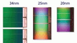
Moore's Law states that computing power on integrated circuits (ICs) grows exponentially — doubling every two years. First observed in 1965, this increase of transistor sensing, memory, and processing capabilities continues unabated. So how do chip engineers consistently cram more functionality onto increasingly tiny chips?
One essential ingredient is motion designs capable of executing the nanoscale tasks required for new chip manufacture.
Conventional mechanical positioners are insufficient, because chip-production mechanisms and motion controls must provide precision 10 to 1,000 times higher than feature size — so error and vibrations must be kept to less than 0.1 nm.
In contrast, piezo-based designs are appropriate: These ceramic solid-state devices convert electrical energy directly into linear motion, so gone are the wear, play, friction, and backlash of rotary-to-linear mechanical elements such as gears and leadscrews. Consider one example pictured above — the N-310 NEXACT PiezoWalk linear drive from Physik Instrumente, Auburn, Mass. The 25 × 25 × 12 mm unit delivers travel to 125 mm and push (or pull) force to 10 N.
However, semiconductor manufacturing and wafer-inspection applications benefit most dramatically from the unit's resolution, so typical for a piezo device: Depending on the drive electronics, open-loop resolution reaches 0.03 nm.
SEMICON West 2011
SEMICON West 2011 will be held July 11 to 14 at the Moscone Center, San Francisco. This annual event showcases new technologies for microelectronics design and manufacturing, including design automation, device fabrication, and manufacturing — including assembly, packaging, and testing. Other topics include micro-electromechanical systems (MEMS), photovoltaics (PV), flexible electronics and displays, nano-electronics, and LEDs. For more information, visit semiconwest.org.
