Synthetic Diamond Manufacturer Feeds Expanding Semiconductor Industry and Emerging Markets
As the semiconductor industry continues to push Moore’s Law, synthetic diamond becomes more critical. There are two common methods of making synthetic diamond. High-pressure high-temperature (HPHT) or chemical-vapor-deposition (CVD) crystal-formation method. Element Six, Luxembourg, a manufacturer of synthetic diamond for over 25 years, offers insight about CVD diamond and the synthetic diamond market. Adrian Wilson, head of the firm’s Technologies Div. says, “Industry demand in semiconductors, optical, sensing and detecting, and waste-water treatment have seen considerable growth over the past year and is expected to continue growing in the coming years. Element Six’s CVD diamond-manufacturing capacity expanded last year by 60% to help meet the growing market demand.”
What is CVD diamond?
Element Six uses a proprietary microwave CVD process to make synthetic diamond. CVD diamond is an engineered material with the highest room-temperature thermal conductivity of any solid. Therefore, when used in semiconductor modules, CVD diamond serves as an effective heat dissipater, addressing the most-common cause of failure in electronics — overheating. Furthermore, CVD diamond heat spreaders and gallium nitride (GaN)-on-diamond wafers let chip designers significantly reduce operating temperatures, extend the operating life, and improve reliability.
The combination of CVD diamond’s ability to dissipate heat with its ability to be transparent at a broad range of wavelengths makes it ideal for optical designers. Optical designers use the material to build systems that operate at much higher powers than those based on materials such as zinc selenide.
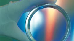
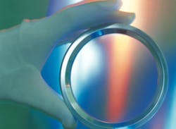
For instance, designers use CVD diamond to make components used in CO2 lasers called windows. The CVD-diamond windows support the semiconductor industry by letting high-power CO₂ lasers drive beyond 6 KW, changing the economics of material processing and opening the door for extreme ultraviolet (EUV) lithography. CVD-diamond windows not only reduce downtime but also improve wafer throughput in EUV lithography. Industry observers predict a significant increase in demand for CVD diamond windows this year because of increasing use of EUV lithography.
New developments and research for CVD diamond
Recent developments and research have created new markets for CVD diamond and could lead to a number of key product developments in 2014 and beyond. One improvement is boron-doped electroanalysis-grade CVD-diamond electrode material. The material was developed by Element Six and is said to be chemically and biologically inert; meaning it can survive in chemical and radioactive environments that would destroy most other materials. The material properties also give it high sensitivity, selectivity, and responsiveness, which make it useful in electroanalysis equipment.
Additionally, recent research breakthrough could also open opportunities for CVD diamond. CVD diamond can now be manufactured with a specific defect — known as a nitrogen vacancy defect. Researchers can use quantum-assisted techniques to control this single defect. By controlling the defect, the material can be used to demonstrate quantum entanglement as a precursor for long-distance encryptions and macro magnetometery.

