Automating Semiconductor Fabrication with Robotics & Wafer Handling Solutions
With demand for chip production on an upswing, the U.S. is on track to triple its chip manufacturing capacity by 2032, according to the Semiconductor Industry Association (SIA).
It follows that this growth can benefit from a robust semiconductor manufacturing ecosystem that supported by an integrated supply chain for advanced tools, clean facilities, precise robotics and metrology that can withstand the rigor needed to produce defect-free chips.
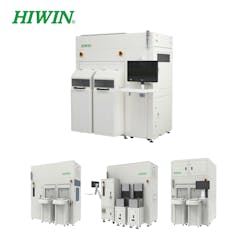
A critical component in this highly controlled equation is the EFEM (equipment front end module). Serving as a central hub for transferring silicon wafers between ultra-clean storage containers and the array of associated processing, inspection and testing systems, EFEMs integrate with robotics, advanced sensors and other critical devices in the fabrication of wafers.
Machine Design had the privilege of a face-to-face meeting Maurice Chang, senior director at HIWIN Technologies Corp., at TIMTOS 2025, a global machine tool show that takes place in Taiwan. In the accompanying video, Chang provides a high-level run through a simulation of wafer production. This demo, highlighting HIWIN’s EFEM (equipment front end module), is just one stage of the otherwise complicated process of wafer production and semiconductor automation in general.
EFEM Integrated with Nano-Level Precision Stage
The demo started at the point where a cassette of wafers was delivered to the EFEM module. The EFEM detects the wafer cassette position via sensors. It controls accuracy at micron level to less than one-tenth of a human hair, said Chang.
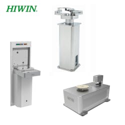
Selecting one wafer at a time, a wafer robot inside the compact cell moves individual wafers. The system supported by a combination of high-precision components produced by HIWIN, explained Chang.
The software and hardware components in the EFEM can be collectively characterized as a vertically integrated control system with flexible options for Wafer ID reading, cassette RFID sensing, wafer protrusion sensing, wafer contour detection and FOUP presence detection. A list of components developed for robot arms include the linear axis stages with ballscrews and guideways, direct drive motors, as well as a laser X-ray or electronic telescope for the processing, Chang said.
Semiconductor Sustainable Manufacturing Development
Semiconductor manufacturing is highly energy intensive. Industry, academia and consortia actively seek sustainable solutions to address the impacts. The semiconductor industry is challenged to improve energy efficiency throughout the lifecycle of microelectronics.
The Taipei International Machine Tool Show (TIMTOS 2025), co-organized by TAITRA and TAMI, took place from March 3-8, 2025. The organizers invited participating semiconductor industry players to explore green manufacturing and net-zero transformation by highlighting sustainable semiconductor manufacturing through their latest technologies.
Participating exhibitors demonstrated measures to reduce carbon emissions along the following criteria:
- Energy management. The ability to optimize cleanroom energy consumption, introduce renewable energy and reduce carbon footprint.
- Water recycling. Advanced water filtration technology to enable a water recycling rate of 95% and reducing water consumption.
- Green materials. Reduce hazardous chemicals, switch to recyclable packaging and meet ESG goals.
READ MORE: Custom Pressure Transducer Delivers High-Temperature Accuracy
TIMTOS 2025 highlighted six major industry trends: precision machine tools, key components, full-scale automation and smart manufacturing, digital twin-driven integration, additive manufacturing and expanded cross-industry applications.
About the Author

Rehana Begg
Editor-in-Chief, Machine Design
As Machine Design’s content lead, Rehana Begg is tasked with elevating the voice of the design and multi-disciplinary engineer in the face of digital transformation and engineering innovation. Begg has more than 24 years of editorial experience and has spent the past decade in the trenches of industrial manufacturing, focusing on new technologies, manufacturing innovation and business. Her B2B career has taken her from corporate boardrooms to plant floors and underground mining stopes, covering everything from automation & IIoT, robotics, mechanical design and additive manufacturing to plant operations, maintenance, reliability and continuous improvement. Begg holds an MBA, a Master of Journalism degree, and a BA (Hons.) in Political Science. She is committed to lifelong learning and feeds her passion for innovation in publishing, transparent science and clear communication by attending relevant conferences and seminars/workshops.
Follow Rehana Begg via the following social media handles:
X: @rehanabegg
LinkedIn: @rehanabegg and @MachineDesign


