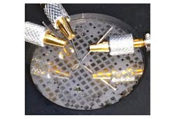
Engineers at the Georgia Institute of Technology have developed a transfer technique based on thin sacrificial layers of boron nitride that could lead to high-performance gallium nitride (GaN) gas sensors being grown on sapphire substrates. The sensors are then removed from substrates and attached to metallic or flexible polymer support materials, which are in turn incorporated into low-cost wearable and disposable sensors for a wide range of environmental and health applications.
Transferring gallium nitride sensors to metallic foils and flexible polymers doubles their sensitivity to nitrogen dioxide gas, boosting response time by a factor of six. The simple production steps, based on metal organic vapor phase epitaxy (MOVPE), could also lower the cost of producing sensors and other optoelectronic devices. Sensors created with the new process detect ammonia at parts-per-billion levels and differentiate between nitrogen-containing gases.
“Mechanically, we just peel the devices off the substrate, like peeling the layers of an onion,” explains Abdallah Ougazzaden, director of Georgia Tech Lorraine in Metz, France and a professor in Georgia Tech’s School of Electrical and Computer Engineering. “We can put the layer on another support that could be flexible, metallic, or plastic. This technique opens up a lot of opportunity for new functionality, new devices, and commercializing them.”
The researchers begin the process by growing monolayers of boron nitride on two-inch sapphire wafers using an MOVPE process at approximately 1,300° C. The boron nitride coating measures only a few nanometers thick, and produces crystalline structures that have strong planar surface connections but weak vertical connections.
Aluminum gallium nitride (AlGaN/GaN) devices are grown atop the monolayers at a temperature of about 1,100° C, also using an MOVPE process. Because of the boron nitride crystalline properties, the devices are attached to substrates only by weak Van der Waals forces, which can be overcome mechanically. The sensors can be transferred to other substrates without inducing cracks or other defects, and the sapphire wafers can be reused for to grow more sensors.
So far, researchers have transferred sensors to copper foil, aluminum foil, and polymer materials. In operation, the sensors differentiate between nitrogen oxide, nitrogen dioxide, and ammonia. Because the devices are approximately 100 by 100 microns, sensors for several gases can be put on a single integrated device.
“Not only can we differentiate between these gases, but because the sensor is small, we can detect them all at the same time with an array of sensors,” says Ougazzaden, who expects the sensors could be modified to also detect ozone, carbon dioxide, and other gases.
The gallium nitride sensors, which are thermally and chemical stable, could have a wide range of applications from industry to vehicle engines—and for wearable sensing devices. “The devices are small and flexible, which will let us put them onto many different types of support,” says Ougazzaden.
To see how transferring the sensors to different substrates affects their performance, researchers measured device performance on the original sapphire wafer and compared it to their performance on the metallic and polymer substrates. They were surprised to see a doubling of sensor sensitivity and a six-fold increase in response time, changes beyond what could be expected by a simple thermal change in the devices.
“Not only can we have flexibility in the substrate, but we can also improve sensor performance just by moving them to different supports with appropriate properties,” Ougazzaden said. “Properties of the substrate alone make the difference in the performance.”
In future work, the researchers hope to boost the quality of the devices and demonstrate other sensing applications. Georgia Tech researchers had previously used a similar technique to create light-emitting diodes and ultraviolet detectors that were transferred to different substrates, and they believe the process could also be used to produce high-power electronics.


