This file type includes high resolution graphics and schematics when applicable.
The environment acting to our whim has been seen in entertainment and may have actually influenced the development of some of today’s inventions. Such science fiction has turned into reality due to the ability of electronics to work with the natural world. However, concerns arise when trying to find the right sensor to detect this world. The following background discussion on sensor manufacturing and a Q&A with experts in the field provides a glimpse of the common issues experienced in the sensor industry.
Special thanks Ian Chen, executive of Freescale’s Sensor Solution Division; Mark Howard, general manager for Zettlex; Tom Curl, managing director at ENERTEX; and Hauke Dierksheide, marketing engineer for First Sensor AG, for shedding some light on common concerns about sensors.
Manufacturing
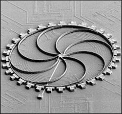
Advances in micromachining and other techniques are generating microstructures that help create more complex sensors with expanded abilities. Processes that foster these complexities and abilities, yet still enable sensors to be mass-produced and economical, are essential to the electronics consumer market.
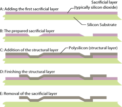
Consider STMicroelectronics’ approach as one case in point. Over the last decade, the company geared itself toward high-volume production with a surface micromachining technique that showed how integrating a sensor, or several, can add more value to a product than the cost of the sensor itself. In general, surface micromachining alternates thin films, often polysilicon and silicon dioxide layered in specific ways. Therefore, when the silicon-dioxide layers, also called the sacrificial layers, are removed by the etchant, it’s possible to leave freestanding structures.
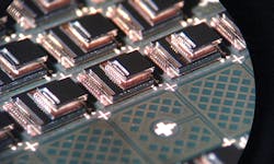
Microelectromechnical-system (MEMS) production is the most common application of the micromachining process. The bulk-method process of micromachining creates multiple electronic elements at the same time, making it preferable for producing larger volumes of sensors and other electronics. Basically, a wafer is masked and then exposed to a chemical etchant for a specific period of time. At this point, the method etches the layer of material not protected by the mask. The process can be repeated several times to form the complex geometries, strategically layer by layer, leading to more powerful sensors.
Electronics may seem synonymous with silicon, but transducers can be made from metals, glass, and even polymers. Certain inherent roadblocks exist with silicon, but its properties, the vast wealth of knowledge about the material, the refined processes for production, and low cost creates an inertia that will keep silicon around for decades to come.
However, Mark Howard predicts that current silicon technology may become less common in high-end devices over the next 10 to 15 years. New materials and hybrids of silicon under development target harsh environments with extreme temperatures and vibrations. Eventually, lower production costs will permit entry to the consumer market.
Wafer bonding—building up of material layers—is another interesting process. Two popular methods involve bonding silicon to silicon or silicon to glass. Technicians can build up layers to team up with micromachining and other processes to add more features to electronic components. This bonding process can also be used to protect an electronic element by adding a layer that seals the unit from the outside environment. Ultimately, it might aid in higher-volume MEMS processing versus current production approaches, and become a driving technology in producing complex forms of electronics.
Sensors Today
Research into designs and processes are helping expand the sensor’s capabilities. The Internet of Things (IoT) and machine-to-machine (M2M) communications are just two examples of the growing demand for electronics that can communicate with the physical world. We asked the experts what technologies we should watch and which were, or might be, game changers.
Ian Chen said, “I have been working in semiconductors and high technology since the late 1980s. I first ran into MEMS in the early 2000s. I would say the continued improvements of size, performance, and cost for MEMS sensors is the biggest advancement I have seen.”
Sometimes the technology isn’t in the sensor itself, but how it is designed. Reducing cost and streamlining the process is also important. Mark Howard talked about his 30-year career as an engineer, and the bigger advances he has seen during that experience.
“Computer-aided drafting is giving designers and engineers the ability to build and even test sensors before cutting any metal. This software is greatly helping to save time and improve sensor quality,” said Howard. “2D and 3D printing are technologies to watch. Giving people the ability to produce low-power, low-cost, miniature integrated circuits, from designing them or adding them into a system from a library and then printing the technology off of a desktop printer, will be a quantum shift.”
The sensor industry is large and many technologies are affecting different markets. When we asked Tom Curl what technologies are leading the industry, he answered, “The answer depends on the industry. Microfluidics in biomedical, MEMS in mechanics/physics, magnetic sensors in machinery, lasers for measurement, carbon nanotube for chemicals, the list can go on and on.”
Many wonder how far electronics will go in terms of power, and what types of features they will possess. Right now, there don’t seem to be any limitations on the electronics and sensor industries as innovations continue unabated. With the IoT, M2M, and wearables, modern electronics can give us applications we might not have thought were possible just five or 10 years ago. Regardless, it’s essential to specify the best sensor for a job. Here are four tips for getting it right:
Select the Right Specifications
Matching demands of an application to properties of a sensor might sound simple enough, and sometimes that’s the case. Sensors cover a wide scope of possibilities, but the more an engineer knows about the process and the types of sensors that are available, the more equipped he or she is to design a system.
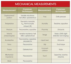
Basic options focus on aligning the product to the nature of the application. Basic properties to look for will change with different sensors, but may include price, size, supply voltage, output signal, and media compatibility.
The first step in this scenario is to match the product’s properties with the application’s demands on the sensor, which helps ensure that the sensor can capture the required signal. The second step is to consider the right technology in the right environment, with the idea of a cradle-to-grave lifespan assigned to the product. Chen said, “More experienced designers might ask about the bandwidth, linearity, and temperature coefficients of a sensor to match their application requirements.”
The sensing industry is rapidly changing, allowing different features to be used in multiple applications. Curl explains, “Early in my career, starting in 1960, detecting if a cooling fan was operational employed a ‘vane switch.’ This was a Microswitch with a thin flat plate facing the vane actuated by the airflow. Later, the job was done optically with LEDs and photodiodes. Today, most cooling fans include built-in magnetic speed sensors to accurately report the rotational speed of the fan. The challenge is trying to find sensors reflecting modern technology at an acceptable cost. This can be difficult in a fast moving industry, as there is almost always something a little better just around the corner.”
Find the Right Signal
Understanding the technology behind how a sensor works can save problems downstream in the manufacturing process, and save time in troubleshooting a system.
“Probably the most interesting challenge in using sensors is to understand what environmental factors will affect the sensor’s readings,” said Chen. “The sensor is measuring the physical world, so it will pick up all the noise in the environment. For example, an accelerometer will also measure gravity. An altimeter will also pick up atmospheric pressure. Pressure is dynamic, changing due to weather. Sensors are very powerful and contain a lot of information, so to distinguish the difference is the most important piece of the puzzle.”
Sensors are sensitive and susceptible to drift. Proper calibration of the sensor and monitoring of electronic components over time is necessary to ensure continued accurate readings. Drift can be caused by the degradation of the sensor’s materials, overuse, and abuse. Customers may not understand the importance of calibration. Manufacturers test and calibrate the sensor, initially, in a closed environment to achieve desired specifications. Once the sensor is in a changed environment, it must be recalibrated.
“The act of soldering a sensor into a circuit can shift the transducer’s offset because it creates a stress the sensor can detect,” said Chen. “The sensor must be calibrated after it is soldered or an algorithm used to negate the offset.”
Once calibrated, the noise or other signals the sensor might detect in the environment must be considered. Designers often reduce noise with signal processing. In one type of signal processing, the first-order derivative from the input signal is recorded and then examined as to how it changes over time. As a result, filters can be added as part of the signal processing to reduce the amount of noise that proceeds to the next step.
Sensor fusion offers another way to reduce noise, and add features. Sensor fusion reduces noise by combining data collected from multiple observers (multiple sensors), and then uses algorithms to compare the data and filter out noise. This technique helps detect the signal desired by the end user, keeping in mind that the end user might be another program, sensor, or machine. Understanding the types of measurements made by the sensor helps engineers select the right sensor for the job. Considering how the sensor measures the environment can also facilitate electronics troubleshooting for technicians.
Nikola Tesla said, “If you want to find the secrets of the universe, think in terms of energy, frequency, and vibration.” Sensors are how engineers are communicating with those energies, frequencies, and vibrations. One could say that the better people communicate with the universe, the more out of this world our innovation in electronics can become.
Consider Environment
Furthermore, environmental concerns aren’t always apparent. Failures have happened to electronics by coastal areas, when components sensitive to salt were not sealed or replaced with a more technology that better handles humid or salty air. Howard added, “It is important to select the most appropriate technology for the application. For example, make sure you’re not putting an optical sensor in a dirty environment where it will get covered in oil and stop working, or a potentiometer in a high-vibration environment where it will wear out after a day.”
Selecting the right sensor that can do the job is foremost, but thinking about the sensor’s capabilities in a particular environment is crucial, too. Selecting inappropriate devices could cost companies millions of dollars from mistakes that, in hindsight, seemed elementary. However, when designing in a controlled environment, it may take an extra step to consider what might seem obvious.
Consider Cost
The bottom line is important in any part of a design. When thinking in terms of mass production of a product, reducing the cost of a single sensor could significantly shrink production costs. However, it’s important to remember that selecting a cheap sensor versus a cost-effective device could wind up hurting the company’s reputation and profit margins.
Howard said, “First, understand the nature of the application. In other words, a solid requirements spec. Second, match the spec to the most appropriate sensor technology. The most frequent question is ‘How much does a sensor cost?’ It is disappointing. Often focusing on a low-cost sensor will result in much higher costs in the end. ‘Most appropriate technology’ means least overall cost; taking everything into consideration, not just the sticker price.”
However, processes like micromachining have had a huge impact on both size and cost. “MEM-based gyros, for example, have replaced spinning mechanical devices, costing hundreds even thousands of dollars with devices costing less than a dollar and having even greater accuracy,” said Curl.
In another example, engineers are using sensor fusion with multiple microphones to determine a sound’s origin. This technology means your smartphone could eventually work with an app to replace hundreds of dollars of audio equipment.
This file type includes high resolution graphics and schematics when applicable.
Reducing cost largely relates to the mass production of sensors and other electronic components. Manufacturing and the market have allowed for this level of production. With all of the available software and platforms, sensor applications are on the rise. And the processes and designs for them, right now, look like they will continue offering more for less.
