Image

The ABCs of LEDs

March 23, 2015
The integration of the inimitable LED into a myriad of lighting applications not only saves energy costs on a mass scale, but the environment from carbon dioxide, too.

Einstein said: “Energy cannot be created or destroyed, it can only be changed from one form to another.” For many light bulbs, this typically means an electrical energy that’s sent through a material—the filament—which heats up. Some of this electrical energy changes into heat and some changes into light.

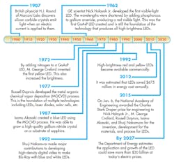
The timeline shows the development stages leading up to the formation of LEDs, and the subsequent advances in the technology.

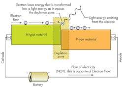
For light-emitting diodes (LEDs), the material is, of course, a diode rather than a filament. A diode, simply put, is a semiconductor that allows electrical current to flow in one direction. One way to make diodes is by doping the conducting material so that it has two regions. There is a p-type, positive region, and an n-type, negative region. An anode attaches to the p-type side and a cathode to the n-type side. When electrons cross over the border where the two regions meet (the p-n junction), some of the electron energy is “lost” or changed into light.

The 49 million LEDs installed in 2012 save an estimated $675 million in energy costs. In 2013, LEDs used in lighting applications throughout the U.S. eliminated more than 12 million tons of CO2 emissions.

LEDs En Masse

It took mass production of LEDs to make the above numbers possible. Following on that theme, several suitable methods have emerged for producing LEDs on a large scale.

A diode connected to a battery forces electrons to “jump” across the depletion zone. As it jumps, it emits electromagnetic energy at a visible frequency.

One of the more common manufacturing methods has technicians making structured 3D semiconductors by first growing a crystal, then slicing and polishing it into a thin wafer, known as the substrate. Layers of crystals are grown on the substrate’s surface and shot with ions to fill gaps in the 3D matrix of the semiconductor. This creates the p- and n-regions.

It has proven more cost-effective from a fabrication standpoint, since thousands of LEDs are made on a single wafer. For example, a 2-in. diameter wafer can yield up to 6,000 LEDs. However, producing a single LED chip from a wafer requires a specialized cutting process, which inevitably reduces the overall yield. Thus, to lower the price of LEDs and semiconductors, a better method is needed to separate them.

The next step in the fabrication process involves coating diodes to form metal contacts, and then connecting two wires to the different sides. Finally, this assembly is placed in a mold, where it gets a protective housing. One of the most common housings is a plastic dome. Housings can also be designed to act as a lens to improve the final LED’s optical qualities.
About the Author

Jeff Kerns | Technology Editor

Studying mechanical engineering at Rochester Institute of Technology (RIT), he worked in the Polymer Research Lab. Utilizing RIT’s co-op program Jeff worked for two aerospace companies focusing on drafting, quality, and manufacturing for aerospace fasteners and metallurgy. He also studied abroad living in Dubrovnik, Croatia. After college, he became a commissioning engineer, traveling the world working on precision rotary equipment. Then he attended a few masters courses at the local college, and helped an automation company build equipment.

Growing up in Lancaster County, PA he always liked to tinker, build, and invent. He is ecstatic to be at Machine Design Magazine in New York City and looks forward to producing valuable information in the mechanical industry. 

Like him on Facebook and follow him on Twitter.

Sponsored Recommendations

Safety Risk Assessment Guidelines for Automation Equipment

Dec. 20, 2024
This Frequently Asked Questions (FAQ) covers the basics of risk assessments, including the goals of the assessment, gathering the right team to perform them, and several methodologies...

Safety Products Overview

Dec. 20, 2024
The collection of machine safeguarding devices from Schmersal include keyed interlocks, solenoid locks, safety sensors, limit switches, safety light curtains and more.

SAFER Workplace: Stop, Assess, Formulate, Execute, Review

Dec. 20, 2024
Our SAFER Workplace initiative promotes workplace safety, with a heightened focus on machine safety, to reduce the potential of near misses, accidents, and injuries. Behaving ...

The advantages of a Built-in Bluetooth Interface for Your Safety Light Curtains

Dec. 20, 2024
Safety Light Curtains with Bluetooth InterfaceGuido Gutmann, Key Account Manager, Optoelectronic Safety Devices, Schmersal Group, explains the advantages of ...

Voice your opinion!

To join the conversation, and become an exclusive member of Machine Design, create an account today!