Ultrasound: Don’t Be Blinded by Your Amplifier’s Slow Overload Recovery
Download this article in PDF format.
Ultrasound receivers are frequently exposed to overload conditions during B-mode and pulsed Doppler operation. These conditions can saturate the amplifiers and/or the analog-to-digital converter (ADC) within the receive amplifier-front-end (AFE) signal chain. An ultrasound receiver with poor overload recovery characteristics can greatly complicate design, significantly reduce image quality, and lengthen time-to-market. This article reviews ultrasound system design challenges with regard to overload recovery, and presents a new approach to address this issue.
The Ultrasound System
Ultrasound has a wide range of medical applications, including imaging, blood flow measurement, cancerous lesion detection, bone densitometry, and needle or catheter guidance.
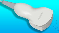
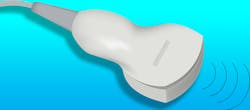
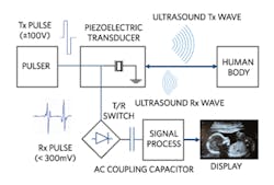
The ultrasound transmitter applies acoustic waves to the body with an ultrasound probe that contains a piezoelectric transducer (Fig. 1), and the ultrasound receiver picks up the echoes reflecting from the body structure, generally by means of the same piezoelectric transducer. Figure 2 is a high-level illustration of the ultrasound system.
1. Ultrasound probe applies acoustic waves to the body.
2. Shown is a high-level ultrasound system setup.
In a pulsed-wave (PW) ultrasound system, a high-voltage pulse stimulates the piezoelectric transducer (a crystal) housed in the ultrasound probe. This causes a corresponding mechanical compression (a reverse piezoelectric effect) and creates the ultrasound compression/relaxation wave that traverses through the body. This wave, focused using phased-array techniques in the lateral plane and through a lens in the elevation plane (see Figure 6 further down), propagates through the body and through the various body substances (soft tissue, bone, fat, and blood). At each substance boundary, a portion of the compression wave is reflected back to the transducer.
Since sound travels at a relatively constant velocity, the delay of the returning pulse represents the distance of the target, while the Doppler frequency shift provides information about the motion of the target. The reflected signal is processed and displayed as an image on a screen. The electric signals to/from the probe are generally processed in the “cart,” a mobile structure including transmitter circuitry, the AFEs, the processing unit, and the display.
The Receiver Channel
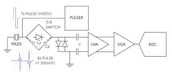
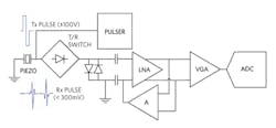
Figure 3 shows the receiver channel in greater detail. The ac signal received through the capacitor bank C is amplified by the low-noise amplifier (LNA) and the variable-gain amplifier (VGA) before being digitalized by the ADC.
3. Ultrasound pulser and receiver chain.
Two back-to-back protection diodes before the input coupling cap C limit the voltage at the receiver input chain. In the presence of large input signals, they can become forward-biased, and the input is held at a VBE(on) above or below ground. These protection diodes are designed so that the VBE(on) voltages, typically about 1 V, are significantly greater than the linear input range of the LNA.
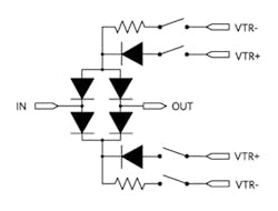
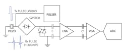
In front of the receiver chain we have the transmit/receive (T/R) switch (Fig. 4), separating the high-voltage transmit signals from the low-voltage receive domain. The T/R switch isolates the receiver during the high-voltage transmission bursts. Traditionally, the TR switch is implemented as a simple diode bridge, biased on during both the transmit and receive intervals. This implementation forces the protection diodes to limit the amplitude of the input signal when the transmitter is active.
4. The transmit/receive (T/R) switch.
Modern pulsers can bias off the bridge during the transmit interval to better isolate the receiver. The T/R switch is closed when the four diodes in the bridge are forward-biased and open when they’re reverse-biased.
Since ultrasound signals are attenuated as they travel through the body, the reflected (received) signal is much smaller than the transmitted signal. Its detectable peak at the input of the LNA is limited by the LNA’s linear input range, typically 500 mV p-p at an LNA gain of 18 dB. Since the received signal is ac, it will ride on top of any offset at the output of the LNA. Such an offset will reduce the LNA’s effective range of operation before saturation. Note that one rail, either the top voltage rail or the bottom voltage rail, will usually saturate before the other.
From the output of the LNA, the ac signal and any offset propagates into a VGA stage or a voltage-controlled attenuator (VCAT) followed by a fixed-gain stage, where the gain (or voltage-controlled attenuation) is programmed to change as a function of time to compensate for the signal attenuation in tissue.
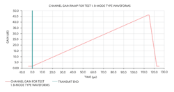
Figure 5 shows the typical time-varying gain profile of the receiver channel for a 3.5-MHz probe. The 120-µs-long gain ramp amplifies the input signal exponentially over time (linearly in dB) to match the attenuating effects of the human body. Thus, the minimally attenuated signals reflected from the near-field tissue (near the front of the gain ramp) will see minimum gains, while the significantly attenuated signals received from the far field (near the back of the gain ramp) will see maximum gains.
5. Here’s a typical receiving-channel gain profile.
Using this technique, signal reflections from deep inside the body (far field) can be picked up and processed by the ultrasound receiver electronics.
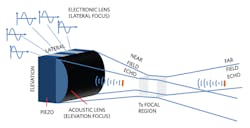
Figure 6 illustrates the echoes from the near and far fields. Low-frequency probes (2- to 3-MHz center frequencies) can typically see reflections from over 20 cm of tissue. (The roundtrip time for signals traveling at the speed of sound is 13 µs/cm or 260 µs for 20 cm). The gain profile assures that the received signals have an amplitude unaffected by distance for a significant duration of a single transmit interval. Naturally, any fixed dc or dynamic offset built up on the input ac coupling capacitor receives the same treatment and is exponentially amplified over time!
6. Near- and far-field echoes.
The Overload Recovery Challenge
Overload conditions can occur during the transmit interval when transmit pulses couple into the receiver input through the transmit/receive (T/R) switch. They may also occur during the receive interval due to large input signals caused by strong reflectors.
During the transmit phase, large signals can be directly coupled into the receiver input or capacitively coupled into the receiver depending on the TR switch architecture. The large transmit coupled signals can directly saturate the receiver or may cause problematic charge buildup on the Rx input coupling capacitors that take a long time to discharge.
The condition can be challenging during transmit events such as B-mode or pulsed-wave Doppler (PWD) bursts and particularly difficult during prolonged elastography push pulses. During these events, current feedthrough partially blinds the receiver by charging the input coupling capacitors (bank C in Figure 3) and limiting the available dynamic range of the receiver.
During the receive interval, strong specular reflections in the near-field can also cause significant overload recovery problems, even when the gain is set low or in the mid-range where the gain is set high. Doppler imaging modes are particularly challenging. The small return signals from blood can sometimes require high receive-chain gain in order to push them above the ADC noise floor, increasing the likelihood of Rx signal-chain saturation from stronger reflections near the area of interest. Saturation conditions within the receiver will temporarily corrupt the digitized results, effectively blinding the receiver after removal of those saturation conditions and while the amplifier recovers.
Each of these overload problems can “blind” the receiver for an extended period of time by reducing the available ADC dynamic range, making it difficult to see small signals in the presence of larger ones or by losing the Rx signal altogether. The blindness will persist until the receive-chain amplifiers and ADCs fully recover.
One important task for designers of ultrasound equipment is to choose an ultrasound Rx AFE that has good overload recovery characteristics. An ultrasound system with fast overload recovery time ensures that minimum valuable information is lost after a saturation event. Stated plainly, it can make the difference between a radiologist successfully spotting a small mass of abnormal tissue in a patient, or properly seeing the vascularization of tissue in difficult-to-image organs such as the kidney or liver, and missing such clues altogether.
Overload from “On” T/R Switch
The transmit signal is often a high-voltage pulse (±100 V) with high slew rate (dV/dt), centered at ground (Fig. 2, again). If the T/R switch remains on during the Tx pulse, with bias current flowing in the diodes, the output will try to follow the input until one of the two back-to-back input protection diodes becomes forward-biased. The input is then held at a fixed VBE(on) above or below ground. Thus, the LNA will go into an overload condition at the beginning of a transmit burst.
Given that it’s important to be able to receive superficial echoes in the near-field as soon as reflections begin to arrive from tissue discontinuities, the LNA and associated input coupling capacitor must be designed to quickly recover from the overload condition. It’s important not to lose information from these returning echoes while the LNA is recovering, and is thus blind until normal linear operation is restored. The round-trip time for a transmit pulse to traverse the lens is typically 2 to 4 µs. Therefore, it’s crucial that the LNA recovers from a strong overload condition in less than 2 µs. A well-designed LNA should recover in 0.6 to 0.8 µs.
CPdV/dt Feedthrough Current
Whether the T/R switch is biased on or off, it has the unfortunate characteristic of having a parasitic capacitance (CP) from its input to output. This is a major problem with diode-bridge-based T/R switches, and a somewhat less significant problem with active T/R switches.
Large transmit pulse swings with fast slew rates and high dV/dt can cause substantial feedthrough current that charges the input ac coupling capacitor. This limits the dynamic range of the receiver by adding a dc error component to the input signal. The dc error component slowly bleeds off the coupling capacitor. Until it bleeds off entirely, the LNA and VGA amplifiers will amplify this error component and present the results to the ADC. The LNA+VGA gain can become quite high, up to 40 dB and beyond.
For instance, if these dV/dt feedthrough currents charge up the input ac coupling capacitor by 10 mV, this would add a 10-mV error component to the ac signal of interest. A 10-mV error with 40 dB of gain will cause a shift of 500 mV in the common-mode signal of the VGA output away from the center of the ADC’s input range. It could then cause one-sided saturation of the ac signal of interest, thus eroding a significant portion of the available ADC dynamic range.
If we closely examine the buildup of charge on the ac input coupling capacitor, we will find that the charge buildup results from one or both of two problems:
Problem 1: Asymmetric transmit pulses where the time duration at the positive voltage is different from the time duration at the negative voltage.
These pulses can cause small mismatches in the LNA input bias currents or in the currents flowing through the devices that set the LNA input common-mode voltage. These current mismatches aren’t necessarily symmetric and will be integrated over different transmit voltage positive and negative duration times. This effectively charges the input ac coupling capacitor and triggers a dc error (offset) voltage at the input of the LNA.
Problem 2: Asymmetric transmit pulses with different rising and falling slew rates at the T/R switch input.
These can also cause ac coupling-capacitor charge mismatches and dc offsets, since asymmetric and opposing CPdV/dt currents through the CP across the T/R switch may not cancel completely (Fig. 2, again). It can take hundreds of microseconds for this charge to bleed off.
This input offset is subsequently amplified by the LNA gain. The LNA gain is generally a fixed value, e.g., 18 dB. Thereafter, the offset is further amplified by the VGA, or a voltage-controlled attenuator followed by a fixed-gain amplifier stage. In B-mode imaging, the VGA gain will increase linearly in dB with time to compensate for tissue-based compression wave attenuation.
Since the signal of interest rides on top of the offset in both amplifying stages (LNA and VGA), there could be significant one-sided saturation within the VGA gain stage as well as significant one-sided over-range condition at the ADC input, as the ADC tends to saturate before the VGA. The use of a dc-blocking digital high-pass filter (DHPF) can generally remove this undesirable offset component from the digitized data, However, using the ADC’s full-scale range is compromised in the process and often necessitates a corresponding reduction in VGA gain to keep the amplifier output stages and the ADC out of saturation.
In other words, in the presence of significant dc offset, for a given image, the ultrasound technician may be forced to reduce the gain to keep the Rx signal chain from saturating. With less gain, some of the small second-harmonic echoes and the small blood echoes will disappear below the noise floor of the ADC, thus deteriorating image quality.
Overload from Transmit Events
Both overload from an “on” T/R switch or overload from CPdV/dt feedthrough current, discussed previously, are associated with transmit events. It’s important that the receiver recovers fully from these overload events in less time than it takes for the compression wave to propagate through the ultrasound lens. In a well-designed receiver, this time should be around 0.6 to 0.8 µs or less.
Overload from Strong Specular Reflections
Additional saturation problems can occur during normal B-mode, tissue harmonic imaging (THI), or during Doppler imaging—PW or color flow (CF) —well after the Tx pulses are finished and receive information is being processed. That is, there can be overload problems due to normal receive events.
Specular reflections from large, smooth tissue boundaries can have echoes of a magnitude large enough to saturate either the LNA or, more frequently, the VGA stages. This happens particularly in the near-field close to the ultrasound probe or from deeper within the tissue when the receive-chain gain is turned up high. It’s important that both the LNA and the VGA of a good ultrasound receiver recover quickly from strong specular reflections. A well-designed receiver under these conditions should recover ideally in 20-25 ns, as it will be temporarily blinded until the recovery is completed.
The phase shift of the signal must be preserved under medium saturation conditions (0 to 6 dB of saturation) to enable Doppler imaging. The receiver recovery performance is particularly important in Doppler imaging, as blood-vessel walls can have relatively strong reflections compared to the red-blood-cell reflections within the vessel. The gain must be turned up to see the small reflections of the blood, creating a situation where the vessel-wall reflections could saturate the LNA/VGA. Without a fast LNA/VGA recovery, the receiver will not be able to see the adjacent blood signals beyond the vessel wall during color-flow imaging.
It should be noted that not only can the LNA/VGA stage be saturated during these specular reflection events, but so too will the ADC that follows them. The ADC should also be designed for a fast recovery from an over-range condition. In a well-designed receiver, only 1 clock cycle (25 ns at 40 MHz) should be needed before the ADC returns to normal operation after a saturation event.
Common Solutions and Their Shortcomings
The LNA and VGA stages, as well as the ADC, should be designed such that they all recover quickly from an overload condition. That’s because the receiver will be effectively blind until the recovery has finished, and image quality can suffer, or the Doppler phase-shift information can’t be preserved.
In dealing with asymmetric CPdV/dt currents building up charge on the input ac coupling capacitor, some solutions either utilize shunt inductors in parallel with the protection diodes, or use a feedback circuit around the LNA to try to compensate for the charge built up during the Tx burst (Fig. 6), or both. In a feedback scheme like that in Figure 7, the input offset caused by the Tx burst is cancelled by injecting a charge in the bottom ac coupling capacitor, developing an offset identical to that of the top capacitor, assuming the system remains linear in the process.
7. A typical offset cancellation scheme.
With this type of a compensation circuit, problems can arise when the LNA strongly saturates. At the same time, there’s a need to keep the feedback loop that corrects for the offset of the input ac coupling capacitor fully operational. During the overload event, the offset feedback circuit is necessarily broken while the LNA is saturated. To make matters worse, during this same overload event, significant charge can be built up across the input ac coupling capacitor. Thus, when the LNA does recover from deep saturation conditions (often a time-consuming process), the offset feedback circuit, which is necessarily in a slow feedback loop, will take yet more time to compensate for any built-up dc offsets, commonly quite significant during such overload events.
To preserve amplifier stability, the offset feedback loop must be much slower than the feedback loop that sets the LNA active input impedance. Therefore, the recovery of both the amplifier and its correction loop must be considered. Overload recovery curves for these types of implementations often show only a VGA (or VCAT+FG) stage recovery, while staying silent about LNA recovery.
A complete representation of the circuit’s overload recovery should show:
- The LNA overload recovery without subsequent saturation of the VGA stage.
- The VGA stage overload recovery.
- Some proof that dynamic range hasn’t been significantly compromised by DC offset build up.
An Ideal Solution
The ideal solution must provide fast recovery of both the LNA and VGA amplifier stages during both the transmit and the receive intervals. Special care needs to be taken with the design of the LNA ac-coupled input stage, as the first stage must be kept out of deep saturation—a condition that can frequently occur around the TX burst and cause notoriously slow recovery times.
Another important feature of a proper solution is to interrupt the dc chain at the output of the LNA by means of a second bank of ac coupling capacitors (C1 in Figure 8). This way, any Tx-burst-related offset is blocked from going to the VGA and getting further amplified, preventing it from limiting the receiver’s dynamic-range performance.
8. This represents an ideal offset cancellation scheme.
The MAX2084 device from Maxim Integrated is an example of a solution that can implement the strategy outlined above. It addresses all critical overload conditions, namely T/R switch in receive mode, input ac coupling-capacitor offset management, strong specular reflections in the near-field, as well as relatively stronger reflections adjacent to smaller blood-cell reflections during Doppler imaging. Further, this receiver doesn’t require additional shunt inductors in parallel with the protection diodes to help manage charge on the input coupling capacitors.
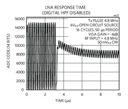
Only one clock cycle is needed before the ADC returns to normal operation after the occurrence of a saturation event. Figure 9 shows the LNA overload recovery time from a large input. In this condition, the LNA recovery time can be seen as the small continuous-wave signal begins to pass through the LNA normally; the recovery time is clearly less than two 4.8-MHz cycles or < 0.4 µs. Note that the decaying signal component is due to the behavior of the analog high-pass filter formed by the ac coupling capacitor and the input impedance of the VGA input stage, which has a time constant of about 1.3 µs and settles within a few microseconds.
9. LNA overload recovery time.
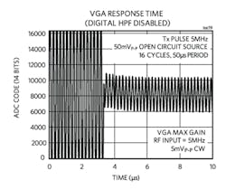
Figure 10 illustrates the VGA overload recovery time from a small input offset. In this condition, the VGA recovery time is about one ADC clock cycle.
10. VGA overload recovery time.
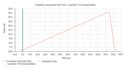
The efficacy of the ac coupling capacitors between the LNA and VGA stages is shown in Figures 11 and 12. Fig. 11 reveals the gain control profile used for a B-mode test, where ±100-V Tx pulses are followed by a receive-chain interrogation. A curvilinear transducer with a 3.5-MHz center frequency is used with a general-purpose ultrasound phantom.
11. Gain profile for full Tx/Rx chain B-mode overload recovery test.
12. Receive data digitized results.
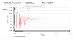
Figure 12 gives the digitized results from the receive chain with the DHPF bypassed during the application of the gain ramp in Fig. 10. As discussed earlier, for normal B-mode time gain control, the receiver gain profile increases exponentially over time (linearly in dB) to match signal-attenuation characteristics of ultrasonic compression waves in tissue. Accordingly, we would expect to see a flat response (centered around the ADC’s zero code) if there were no residual problems with Tx-burst induced offsets.
Conversely, if there were any offset problems, you would see the ADC code increase exponentially as the gain increased over time. This clearly isn’t the case with the results shown in Fig. 11, where the flatness of the curve indicates absence of offset. A full overload recovery report is available, showing good recovery performance with even more challenging gain profiles, such as those used in color flow or even more challenging Tx-burst conditions, such as for elastography. Contact Maxim Design Support for more information.
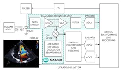
The IC includes an octal continuous-wave Doppler (CWD) beamformer for a full Doppler solution (Fig. 13).
13. Integrated ultrasound receiver with T/R switch.
Conclusion
The causes and effects of overload in the ultrasound receiver chain during transmit and receive intervals were discussed in detail, and the shortcomings of current solutions were highlighted. Introduced were a new solution that implements fast recovery amplifiers, and a new technique that manages offset error generated from the Tx burst by placing ac coupling capacitors between the LNA and the VGA.
This solution prevents the offset error from propagating to the VGA stage. The end result is a substantial improvement in dynamic-range performance for the entire receive interval, after the initial Tx-burst-related LNA saturation and input ac coupling capacitor charge build up. Thus, overload induced blind spots are minimized during imaging.
Choosing an ultrasound receiver with good overload recovery characteristics can greatly simplify HW/SW design and debug challenges, speeding up time-to-market and considerably enhancing image quality.
Jim Chapman is Principal MTS and Nazzareno (Reno) Rossetti is Analog and Power Management Expert at Maxim Integrated.
