A kind of electrical inertia, inductance is a circuit’s ability to store energy in electromagnetic fields. Straight wire generates miniscule inductance while wound wire builds more, because magnetic forces align and multiply to resist changes in current. When charged with current, coils can produce substantial countering electromotive force.
Some software is giving engineers a better, more efficient way to probe engineering material properties. By using analytical calculations and then exporting automatically generated geometry directly into software, users can avoid the construction of physical models and quickly determine magnetic fields, current distributions, and the magnetic flux density of their system. By assigning currents to objects in magnetostatic, Eddy current, and transient analyses with boundary manager features, users can make good estimations of their design’s performance. From there, some software even determines force, torque, inductances, and saturation.
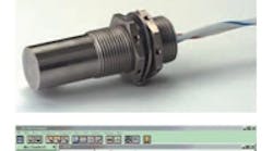
One such program from Ansoft Corp. of Pittsburgh was developed specifically for the design and testing of electromagnetic components. At ELDEC Corp., an electronic sensor company based in Lynnwood, Wash., engineers have been using Ansoft’s Maxwell software with their own mapping method to design their proximity sensors. Geometry information is entered directly into the Maxwell modeler, which makes subsequent Eddy current readings and analysis quicker. This is especially helpful in situations where sensors are constructed of materials with under-documented conductivity or permeability characteristics; these characteristics vary with temperature, which is a concern in aerospace and defense applications. Before using simulation software, ELDEC material selections were best guesses, and were verified by time-consuming toroid construction. Because of the difficulties involved in reiteration, the shape of their sensors also received little optimization.
Cool mist
Die-casting has made many improvements, but one thing has remained the same — the costly time between a design order and production. Two major bottlenecks include the need to make prototypes with slower methods — usually sand-casting — and the tooling lead-time after prototypes are approved.
Rapid solidification process or RSP tooling is an emerging method that speeds the cycle. Originally developed by the Idaho National Engineering and Environmental Laboratory, RSP Tooling LLC based in Solon, Ohio, now markets the process as a prototyping and production method. The process begins with a CAD model of a part to be produced. From this model, a tooling master is made with a rapid prototyping method (such as stereolithography). From it a pattern transfer is made to a castable ceramic, usually in a vacuum chamber to avoid air bubbles or other deformities. Alumina or fused silica is used for the ceramic mold negative; this piece is then attached to a spinning system member that sits in the direct spray stream of molted metal. After enough metal has been sprayed and the mold filled, the part is cooled, removed, and its edges cleaned for use. Sprayed, the material has a hardness of 59 HRC. Age hardening can increase this to 62 HRC.
Heat treatment changes mechanical properties and metallurgical structures of metals, and improves their strength. Solution heating at a specified temperature dissolves soluble phases. Then quenching in a fluid changes the metal to a supersaturated form. Finally, age hardening precipitates solute atoms. Sometimes metals are also tempered by reheating to achieve required mechanical properties. Upon slow cooling, phases reform.
